Strategic collaborations with Samsung Foundry, Arm and others enable Cadence to deliver pre-validated chiplet solutions based on the Cadence Physical AI chiplet platform
Cadence (Nasdaq: CDNS) today announced a Chiplet Spec-to-Packaged Parts ecosystem to reduce engineering complexity and accelerate time to market for customers developing chiplets targeting physical AI, data center, and high-performance computing (HPC) applications. Initial IP partners joining Cadence include Arm, Arteris, eMemory, M31 Technology, Silicon Creations and Trilinear Technologies, as well as silicon analytics partner proteanTecs. To help reduce risk and streamline customer adoption, Cadence is collaborating with Samsung Foundry to build out a silicon prototype demonstration of the Cadence® Physical AI chiplet platform, including pre-integrated partner IP on the Samsung Foundry SF5A process.
This press release features multimedia. View the full release here: https://www.businesswire.com/news/home/20260106077060/en/
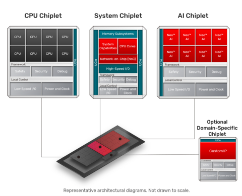
Cadence's Chiplet Spec-to-Packaged Parts ecosystem reduces engineering complexity and accelerates time to market for customers developing chiplets targeting physical AI, data center, and HPC applications.
Extending their longstanding history of close collaboration, Cadence and Arm are working together to accelerate innovation across physical and infrastructure AI applications. Cadence will leverage the advanced Arm® Zena™ Compute Subsystem (CSS) and other essential IP to enhance Cadence’s Physical AI chiplet platform and Chiplet Framework. The resulting new Cadence solutions accommodate the demanding next-generation edge AI processing requirements for automobiles, robotics and drones, as well as the needs of standards-based I/O and memory chiplets for data center, cloud and HPC applications. The alliances reduce engineering complexities, offer customers a low-risk path to advanced chiplet adoption and pave the way for smarter, safer and more efficient systems.
“Cadence’s new chiplet ecosystem represents a significant milestone in chiplet enablement,” said David Glasco, vice president of the Compute Solutions Group at Cadence. “Multi-die and chiplet-based architectures are increasingly critical to achieving greater performance and cost efficiency amid growing design complexity. Cadence’s chiplet solutions optimize costs, provide customization flexibility and enable configurability. By combining our extensive IP and SoC design expertise with pre-integrated and pre-validated IP from our robust partner ecosystem, Cadence is accelerating the development of chiplet-based solutions and helping customers mitigate risk to quickly realize their chiplet ambitions with greater confidence.”
Cadence has built spec-driven automation to generate chiplet framework architectures that combine Cadence IP and third-party partner IP with chiplet management, security, and safety features, all supported by advanced software. The generated EDA tool flow enables seamless simulation with the Cadence Xcelium™ Logic Simulator and emulation with the Cadence Palladium® Z3 Enterprise Emulation Platform, while the physical design flow employs real-time feedback for efficient place-and-route cycles. The resulting chiplet architectures are standards-compliant to ensure broad interoperability across the chiplet ecosystem, including adherence to the Arm Chiplet System Architecture and future OCP Foundational Chiplet System Architecture. Cadence’s Universal Chiplet Interconnect Express™ (UCIe™) IP provides industry-standard die-to-die connectivity, while a comprehensive protocol IP portfolio enables fast integration of leading-edge interfaces such as LPDDR6/5X, DDR5-MRDIMM, PCI Express® (PCIe®) 7.0, and HBM4.
An earlier prototype of the Cadence base system chiplet, which is part of the Cadence Physical AI chiplet platform and incorporates the Cadence chiplet framework, UCIe 32G, and LPDDR5X IP, has already been fully silicon validated.
Supporting Partner Quotes
“As compute demands surge across automotive, robotics, and other emerging applications, the industry needs scalable solutions that deliver higher performance, greater efficiency, and functional safety by design. By leveraging Arm Zena CSS, Cadence’s chiplet platform will meet the requirements of next-generation intelligent systems that will advance the physical AI landscape, accelerate chiplet adoption, and help customers reduce design complexity.”
Suraj Gajendra, Vice President of Products and Solutions, Physical AI Business Unit, Arm
“Arteris network-on-chip IP products, including Ncore and FlexNoC, are at the forefront of innovation, and we are pleased to support the Cadence Physical AI Chiplet Platform and Chiplet Framework. Together with Cadence, we are enabling customers to confidently adopt chiplet architectures with high-bandwidth, scalable, and production-proven interconnect technology for next-generation multi-die systems.”
Guillaume Boillet, Vice President of Strategic Marketing, Arteris
“eMemory’s enhanced OTP products complement Cadence’s Securyzr™ Root of Trust within the Cadence Chiplet Framework. As a leading provider of non-volatile memory technologies, the combination of eMemory technology and Cadence’s security subsystem results in a Physical AI Chiplet platform delivering secure storage and long-lifecycle key management, reinforcing the strong hardware foundation provided by Cadence for die-to-die security and safety in advanced chiplet designs.”
Charles Hsu, Chairman, eMemory
“M31 is proud to be a contributor to Cadence’s expanding chiplet ecosystem, continuously advancing interface IP on leading-edge process technologies and keeping pace with the latest MIPI standards. With proven automotive-grade IP and over a decade of experience supporting high-volume consumer applications, M31 delivers world-class MIPI PHY interface IP that enables customers to rapidly realize advanced chiplet solutions with flexible MIPI CSI and DSI integration.”
Scott Chang, CEO, M31 Technology
“We’re thrilled to partner with Cadence on its chiplet platform, embedding proteanTecs telemetry across all chiplet types. Together we’re enabling safe, reliable and power-efficient physical AI for next-gen compute demands. It’s an amazing collaboration delivering real value for customers building advanced SoCs and systems for automotive and autonomous applications.”
Ziv Paz, VP of Business Development, proteanTecs
“We’re pleased to collaborate with Cadence to demonstrate the competitiveness of Samsung’s SF5A technology. Through this trusted partnership, we look forward to the successful expansion of the Chiplet Spec-to-Packaged Parts ecosystem and helping customers accelerate reliable paths to cutting-edge silicon solutions for physical AI applications, including next-generation automotive designs.”
Taejoong Song, Vice President of Foundry Technology Planning, Samsung Electronics
“As a long-time Cadence partner, we’re pleased to deepen our collaboration through the Chiplet Spec-to-Parts initiative. Over the past 15 years, we’ve developed and delivered over 100 custom PLLs for Cadence across leading foundries. Throughout this partnership, we have provided high-performance low-jitter PLLs and specialized clocking solutions, and we're excited to extend our collaboration to help accelerate next-generation chiplet-based designs.”
Pawel Banachowicz, PLL Product Line Development Director, Silicon Creations
“Trilinear Technologies is excited to provide our advanced DisplayPort IP as part of this innovative initiative. Collaborating with Cadence enables us to drive high-performance video connectivity and deliver flexible, future-ready display solutions for the chiplet ecosystem.”
Carl Ruggiero, CEO, Trilinear Technologies
Related Resources
- eBook: Helping You Realize Your Chiplet Ambitions
- Blog: From Spec to Silicon: Successful Physical AI System Chiplet Bring-Up
- Webinar: Chiplets Solutions: Helping You Realize Your Chiplet Ambitions
- Blog: Cadence Transforms Chiplet Technology with First Arm-Based System Chiplet
- Blog: Jumpstarting the Automotive Chiplet Ecosystem
About Cadence
Cadence is a market leader in AI and digital twins, pioneering the application of computational software to accelerate innovation in the engineering design of silicon to systems. Our design solutions, based on Cadence’s Intelligent System Design™ strategy, are essential for the world’s leading semiconductor and systems companies to build their next-generation products from chips to full electromechanical systems that serve a wide range of markets, including hyperscale computing, mobile communications, automotive, aerospace, industrial, life sciences and robotics. In 2024, Cadence was recognized by the Wall Street Journal as one of the world’s top 100 best-managed companies. Cadence solutions offer limitless opportunities—learn more at www.cadence.com.
© 2026 Cadence Design Systems, Inc. All rights reserved worldwide. Cadence, the Cadence logo and the other Cadence marks found at www.cadence.com/go/trademarks are trademarks or registered trademarks of Cadence Design Systems, Inc. Arm and Zena are registered trademarks or trademarks of Arm Limited (or its subsidiaries) in the US and/or elsewhere. PCI Express and PCIe are registered trademarks of PCI-SIG. Universal Chiplet Interconnect Express and UCIe are trademarks of the UCIe Consortium. All other trademarks are the property of their respective owners.
Category: Featured
View source version on businesswire.com: https://www.businesswire.com/news/home/20260106077060/en/
By combining our extensive IP and SoC design expertise with pre-integrated and pre-validated IP from our robust partner ecosystem, Cadence is accelerating the development of chiplet-based solutions and helping customers mitigate risk.
Contacts
For more information, please contact:
Cadence Newsroom
408-944-7039
newsroom@cadence.com