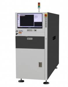
Single Lane - SPC Statistical Process Control - Germany IDS 5.3M Pixel -Machine Customisation is available 3D SPI Specification: Model EKT-8060A Board Handling PCB Size Min: 55*55mm – Max: 400*350mm PCB Thickness 0.6-5.0mm <5.Okg PCB clamping edge clearance 3mm Minimum inspection component 01005 Paste height range 0-500um PCB clearance
EKTION TECHNOLOGY, a leading electronics manufacturing services provider, announces the most recent capital investment in printed circuit board inspection technology and equipment. Final equipment installation and training was recently completed incorporating 3D imaging technology at its Nashville facility with the addition of Solder Paste Inspection and 3D Automated Optical Inspection Systems.
Electronics manufacturing industry standards estimate approximately 70% of surface mount technology (SMT) process-related defects originate from the solder paste printing process. Though most all SMT screen printing systems at a minimum incorporate 2D AQL selective inspection capability, having newly installed 3D solder paste inspection (SPI) verifies not only area (L/W) coverage of paste, but also analyzes third dimension volumetric deposition of solder paste. Adding this capability as an inline standalone machine directly behind the printer reduces the screen printer cycle time while also enabling 100% 3D real time total board paste inspection, stopping the process and prompting immediate operator process engagement and equipment adjustment as necessary.
Additionally, once 3D SPI process verification has been assured, populated circuit board post reflow 3D Automated Optical Inspection (AOI) capability now validates not only 2D component placement accuracy related to presence, X/Y alignment, orientation and character recognition, but also enables third dimension imaging to verify Z-height factors including coplanarity, lifted leads, discrete SMD head-in-pillow (HiP), bridging, and overall solder joint integrity (insufficient or excess).
Final equipment installation and training was recently completed incorporating 3D imaging technology with the addition 3D Solder Paste Inspection and 3D Automated Optical Inspection Systems.
Standardizing on equipment supports business continuity factors where transition between locations adds value, and also facilitates collaboration among production and engineering staff at both sites further encouraging achievement of one of EKTION TECHNOLOGY Fundamental Pillars of Success, a Team Oriented Workforce!
Media Contact
Company Name: EKTION (SHENZHEN) TECHNOLOGY LIMITED
Contact Person: Media Relations
Email: Send Email
Phone: +86-755-27321258
Country: China
Website: https://www.aoiekt.com/
