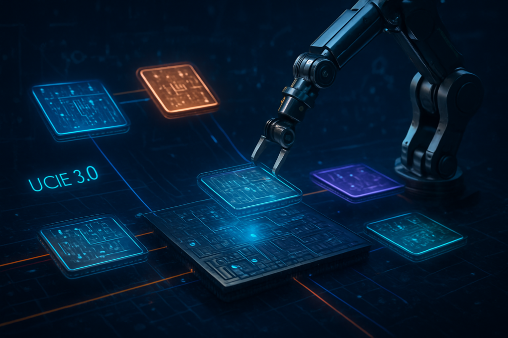
The semiconductor industry has reached a pivotal turning point as the Universal Chiplet Interconnect Express (UCIe) standard enters full commercial maturity. As of late 2025, the release of the UCIe 3.0 specification has effectively dismantled the era of monolithic, "black box" processors, replacing it with a modular "mix and match" ecosystem. This development allows specialized silicon components—known as chiplets—from different manufacturers to be housed within a single package, communicating at speeds that were previously only possible within a single piece of silicon. For the artificial intelligence sector, this represents a massive leap forward, enabling the construction of hyper-specialized AI accelerators that can scale to meet the insatiable compute demands of next-generation large language models (LLMs).
The immediate significance of this transition cannot be overstated. By standardizing how these chiplets communicate, the industry is moving away from proprietary, vendor-locked architectures toward an open marketplace. This shift is expected to slash development costs for custom AI silicon by up to 40% and reduce time-to-market by nearly a year for many fabless design firms. As the AI hardware race intensifies, UCIe 3.0 provides the "lingua franca" that ensures an I/O die from one vendor can work seamlessly with a compute engine from another, all while maintaining the ultra-low latency required for real-time AI inference and training.
The Technical Backbone: From UCIe 1.1 to the 64 GT/s Breakthrough
The technical evolution of the UCIe standard has been rapid, culminating in the August 2025 release of the UCIe 3.0 specification. While UCIe 1.1 focused on basic reliability and health monitoring for automotive and data center applications, and UCIe 2.0 introduced standardized manageability and 3D packaging support, the 3.0 update is a game-changer for high-performance computing. It doubles the data rate to 64 GT/s per lane, providing the massive throughput necessary for the "XPU-to-memory" bottlenecks that have plagued AI clusters. A key innovation in the 3.0 spec is "Runtime Recalibration," which allows links to dynamically adjust power and performance without requiring a system reboot—a critical feature for massive AI data centers that must remain operational 24/7.
This new standard differs fundamentally from previous approaches like Intel Corporation (NASDAQ: INTC)’s proprietary Advanced Interface Bus (AIB) or Advanced Micro Devices, Inc. (NASDAQ: AMD)’s early Infinity Fabric. While those technologies proved the viability of chiplets, they were "closed loops" that prevented cross-vendor interoperability. UCIe 3.0, by contrast, defines everything from the physical layer (the actual wires and bumps) to the protocol layer, ensuring that a chiplet designed by a startup can be integrated into a larger system-on-chip (SoC) manufactured by a giant like NVIDIA Corporation (NASDAQ: NVDA). Initial reactions from the research community have been overwhelmingly positive, with engineers at the Open Compute Project (OCP) hailing it as the "PCIe moment" for internal chip communication.
The Competitive Landscape: Giants and Challengers Align
The shift toward a standardized chiplet ecosystem is creating a new hierarchy among tech giants. Intel Corporation (NASDAQ: INTC) has been the most aggressive proponent, having donated the initial specification to the consortium. Their recent launch of the Granite Rapids-D (Xeon 6 SoC) in early 2025 stands as one of the first high-volume products to fully leverage UCIe for modularity at the edge. Meanwhile, NVIDIA Corporation (NASDAQ: NVDA) has adapted its strategy; while it still champions its proprietary NVLink for high-end GPU clusters, it recently released "UCIe-ready" silicon bridges. These bridges allow customers to build custom AI accelerators that can talk directly to NVIDIA’s Blackwell and upcoming Rubin architectures, effectively turning NVIDIA’s hardware into a platform for third-party innovation.
Taiwan Semiconductor Manufacturing Company (NYSE: TSM) and Samsung Electronics (KRX: 005930) are currently locked in a "foundry race" to provide the packaging technology that makes UCIe possible. TSMC’s 3DFabric and Samsung’s I-Cube/X-Cube technologies are the physical stages where these mix-and-match chiplets perform. In mid-2025, Samsung successfully demonstrated a 4nm chiplet prototype using IP from Synopsys, Inc. (NASDAQ: SNPS), proving that the "mix and match" dream is now a physical reality. This benefits smaller AI startups and fabless companies, who can now purchase "silicon-proven" UCIe blocks from providers like Cadence Design Systems, Inc. (NASDAQ: CDNS) instead of spending millions to design proprietary interconnect logic from scratch.
Scaling AI: Efficiency, Cost, and the End of the "Reticle Limit"
The broader significance of UCIe 3.0 lies in its ability to bypass the "reticle limit"—the physical size limit of a single silicon wafer die. As AI models grow, the chips needed to train them have become so large they are physically impossible to manufacture as a single piece of silicon without massive defects. By breaking the processor into smaller chiplets, manufacturers can achieve much higher yields and lower costs. This fits into the broader AI trend of "heterogeneous computing," where different parts of an AI task are handled by specialized hardware—such as a dedicated matrix multiplication die paired with a high-bandwidth memory (HBM) die and a low-power I/O die.
However, this transition is not without concerns. The primary challenge remains "Standardized Manageability"—the difficulty of debugging a system when the components come from five different companies. If an AI server fails, determining which vendor’s chiplet caused the error becomes a complex legal and technical nightmare. Furthermore, while UCIe 3.0 provides the physical connection, the software stack required to manage these disparate components is still in its infancy. Despite these hurdles, the move toward UCIe is being compared to the transition from mainframe computers to modular PCs; it is an "unbundling" that democratizes high-performance silicon.
The Horizon: Optical I/O and the 'Chiplet Store'
Looking ahead, the near-term focus will be on the integration of Optical Compute Interconnects (OCI). Intel has already demonstrated a fully integrated optical I/O chiplet using UCIe that allows chiplets to communicate via fiber optics at 4TBps over distances up to 100 meters. This effectively turns an entire data center rack into a single, giant "virtual chip." In the long term, experts predict the rise of the "Chiplet Store"—a commercial marketplace where companies can buy pre-manufactured, specialized AI chiplets (like a dedicated "Transformer Engine" or a "Security Enclave") and have them assembled by a third-party packaging house.
The challenges that remain are primarily thermal and structural. Stacking chiplets in 3D (as supported by UCIe 2.0 and 3.0) creates intense heat pockets that require advanced liquid cooling or new materials like glass substrates. Industry analysts predict that by 2027, more than 80% of all high-end AI processors will be UCIe-compliant, as the cost of maintaining proprietary interconnects becomes unsustainable even for the largest tech companies.
A New Blueprint for the AI Age
The maturation of the UCIe standard represents one of the most significant architectural shifts in the history of computing. By providing a standardized, high-speed interface for chiplets, the industry has unlocked a modular future that balances the need for extreme performance with the economic realities of semiconductor manufacturing. The "mix and match" ecosystem is no longer a theoretical concept; it is the foundation upon which the next decade of AI progress will be built.
As we move into 2026, the industry will be watching for the first "multi-vendor" AI chips to hit the market—processors where the compute, memory, and I/O are sourced from entirely different companies. This development marks the end of the monolithic era and the beginning of a more collaborative, efficient, and innovative period in silicon design. For AI companies and investors alike, the message is clear: the future of hardware is no longer about who can build the biggest chip, but who can best orchestrate the most efficient ecosystem of chiplets.
This content is intended for informational purposes only and represents analysis of current AI developments.
TokenRing AI delivers enterprise-grade solutions for multi-agent AI workflow orchestration, AI-powered development tools, and seamless remote collaboration platforms.
For more information, visit https://www.tokenring.ai/.